


Contributors
Subscribe to our newsletter
The Energy Dispersive Spectroscopy (EDS) functionality of the Thermo Axia ChemiSEM instrumentation is a powerful tool in understanding the compositional complexity of samples under analysis. The positional precision of these measurements can be useful in distinguishing different phases in metallurgical samples or identifying different species of particulate in environmental samples. However, even with computer control of the functions of the microscope, the operator needs to be aware of electron beam / sample interactions that can influence the accuracy of those analyses.
There are a variety of artifacts that operators typically encounter during analysis related to the electrical charge associated with bombarding the sample with electrons in the incident beam. A “charging” surface condition typically occurs when a non-conductive material is analyzed or non-conductive particulate settles onto the surface of an otherwise conductive sample (Figure 1).
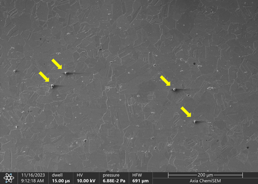
Figure 1. Charging of non-conductive particles settled on surface of
conductive metallurgical sample. (Magnification: 300x)
The shadowing associated with the deflection of the incoming beam due to the increasingly negative electrical charge of the non-conductive material makes imaging and EDS analysis in the vicinity of such a particle impossible under typical analytical conditions. There are a variety of operational strategies – which will be the subject of a future technical note – to overcome this well-known artifact including coating the sample with carbon or operating the microscope in variable pressure.
A perhaps more challenging operational artifact is electron beam drift, which occurs when the sample or stage is not sufficiently grounded to allow passage of the incoming electrons through the sample. Like the surface charging condition mentioned above, electron beam drift is caused by the local buildup of negative charge causing the incoming beam to drift or deflect. However, unlike charging, the operator is not alerted to a problem through local brightness differences or shadowing from a non-conductive particle. Rather, the image will move – sometimes subtly, sometimes significantly – with each raster pass despite no stage movement or intentional beam shift.
This is particularly a concern at high magnifications where the beam is focused on a small area of the sample leading to localized charging issues. Electron beam dwell time on an area for the purposes of high-resolution imaging or EDS analysis can result in features of interest appearing to “march” across the screen. In the Thermo Axia ChemiSEM where magnifications in the 30,000x – 50,000x range and higher are readily achievable, this artifact must be recognized and addressed if present.
Even with the use of some of the charging mitigation steps mentioned previously, electron beam drift can be an issue. Experienced electron microscopists and technicians can address this during imaging by controlling the electron beam through reduction of accelerating voltage or beam current. Reducing the beam dwell time in the imaging area by increasing the raster speed can also be helpful, but that also tends to reduce the resolution of the collected image. EDS analysis presents a much more difficult challenge if electron beam drift is occurring.
Since the microscopist does not have a live image during EDS analysis, it is much more difficult to detect a drift issue. As shown in Figure 2, ghost images in the SEM image are visible only after the compositional mapping is complete (or underway for some period).
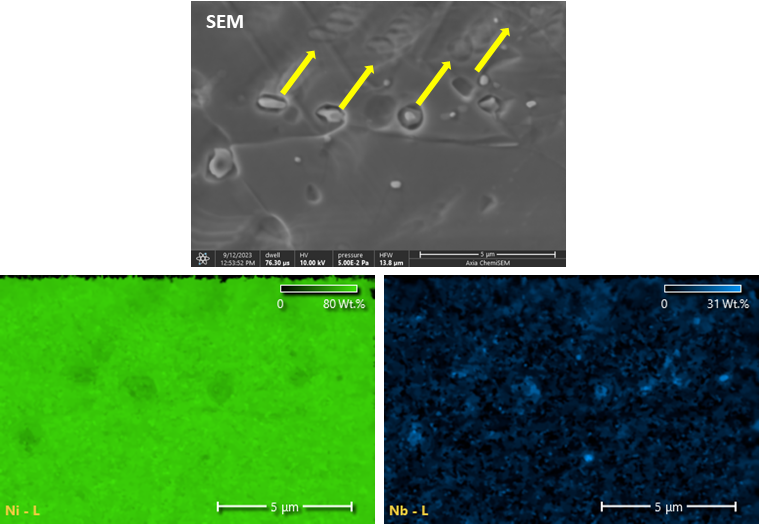
Figure 2. EDS compositional mapping of a polished metallurgical sample with ghost images of precipitates (top) and poor compositional resolution in the elemental maps for nickel (bottom left) and niobium (bottom right). (Magnification: 15,000x)
Point analysis presents an even bigger conundrum as individual points or areas are identified at the start of the analysis (Figure 3). The only way to detect whether there is an issue is to take an image at the conclusion of the analysis to see if there has been a shift such that the points of analysis are no longer in the intended positions.
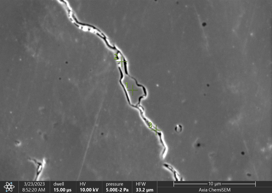
Figure 3. EDS point analysis of secondary phases in a metallurgical sample with
three pointsof analysis identified using crosshairs. (Magnification: 5,000x)
For this reason, some models of the Thermo Axia ChemiSEM are equipped with a drift correction capability that can be used during compositional mapping such that the beam controls compensate for any beam drift that is detected during analysis. The user should note that this option is not available on all Thermo Axia SEM models and this setting needs to be turned on when defining the parameters for EDS mapping.
Drift correction is not available for point analyses, but maps with drift correction can be queried after collection and spectra from specific points or areas can be extracted from the collected maps.
The resolution of extracted spectra will depend on the number of pixels selected and the resolution of the map collected. Optimization of those parameters will be the subject of a future technical note. However, operators should understand that vigilance is still necessary when performing EDS mapping using the drift correction feature; there are limitations to its ability to maintain the intended field of analysis.
If there is insufficient contrast in the field of view to enable the microscope to identify features to maintain positioning the drift correction may not work as intended. Particularly severe electron beam drift can also defeat the drift correction capability such that an EDS mapping analysis runs smoothly for the first several frames followed by a “leap” in position where visible features appear to shift positions significantly (Figure 4). Adjustment of the mapping parameters to reduce the dwell time per frame was found to be a useful tool to avoid recurrence during re-analysis.
This technical note is offered as a reminder of some of the artifacts that microscopists may encounter during analysis and to highlight methods useful in the collection of accurate and reliable data. Even with the aid of computer algorithms to solve some of the challenges with electron beam drift, no correction method is infallible. Vigilance during operation and careful data review and interpretation remain essential aspects of getting the best scientific data from the electron microscope.
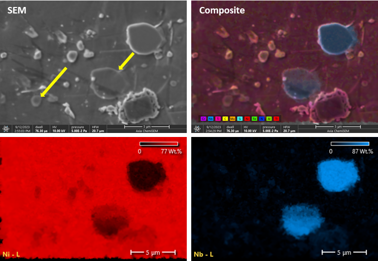
Figure 4. EDS compositional mapping of a polished metallurgical sample with ghost images of precipitates (top) and ghost elemental maps for the composite image (top right), nickel (bottom left) and niobium (bottom right). (Magnification: 10,000x)